Organic semiconductors (OSCs) are promising advanced materials owing to their many attractive properties including their lightweight, mechanical flexibility and processability (low-cost production, low-temperature processing) [1]. They have thus interesting prospects for use in various applications such as organic light-emitting diodes, organic transistors, sensors and biosensors, thin film batteries or organic photovoltaics (OPVs) [2]. Intrinsic drawbacks however prevent them from being used at a larger scale at the moment.
Even though organic solar cells, for example, attain efficiencies comparable to their inorganic (silicon) counterparts (above 18%), the manufacturing processes for this state-of-the-art photovoltaics are not compatible with large-scale production. Using mass production methods, such as roll-to-roll coating, materials of lower performance are obtained (5-10% efficiency) [3]. Improving the understanding of these limitations and developing new production methods is thus an essential step that has been receiving increasing attention from the scientific community.
Recently, a group of researchers from the Technical University of Denmark, the Deutsches Elektronen-Synchrotron (DESY) and the Jülich Centre for Neutron Science (JCNS) at Heinz Maier-Leibnitz Zentrum (MLZ) proposed a method of manipulating the morphology (and implicitly the physical properties) of one such organic semiconductor using visible light during roll-to-roll slot-die coating [3]. Their research focused on the conjugated polymer poly(3-hexylth-iophene) (P3HT) that is often used as an electron donor material in donor-acceptor heterojunctions for OPVs.
Conjugated polymers in general, and P3HT thin films in particular, exhibit changes in their morphology when illuminated with visible light. These structural changes in turn induce modifications of the electric and physical properties of the films.
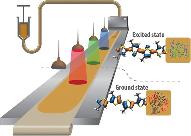
Fig. 1 Illustration of the manufacturing method where poly(3-hexylth-iophene) is slot-die coated on a moving substrate in dark or while illuminated with red, green or blue light. Credit: Adv. Funct. Mater., 2023, DOI: 10.1002/adfm.202212835
As depicted in Figure 1, when excited during coating with visible light, P3HT will transition from a ground state to an excited one. The main structural difference between these two states is represented by the value of the dihedral angles between neighbouring thiophene rings. While the ground state adopts twisted geometries, the excited states are perfectly planar. To study the morphological changes induced by four different light treatments (with energies below and above the excitation energy levels of P3HT) the researchers performed grazing incidence wide angle X-ray scattering (GIWAXS) measurements. Grazing incidence X-ray scattering measurements have already played a significant role in understanding the morphology of active materials and thin film layers used in OPVs [4].
Light-induced changes in the morphology of organic semiconductors as studied by GIWAXS
GIWAXS is a highly effective method that is commonly used to determine the alignment of the polymer chains (backbone orientation) in thin films that have been deposited onto substrates. Figure 2 (a) depicts the common patterns that can be observed in 2D GIWAXS for the coexistence of edge-on and face-on orientation motifs. In the edge-on orientation, the chain backbone is aligned parallel to the substrate together with the π-π stacking direction, while the side chains are perpendicular to the substrate. On the other hand, in the face-on orientation, the π-π stack is directed perpendicularly to the substrate and both the side chains and the chain backbone are aligned in the plane of the substrate. These different orientations have an impact on the electrical properties, as it will be discussed further, and are important to consider when designing and optimizing P3HT-based devices [4]. As an example an extract of two dimensional GIWAXS patterns recorded in the case of this study are shown in Figures 2 (b,c) indicating that the P3HT exhibits a predominantly edge-on orientation with some degree of orientation distribution [3].
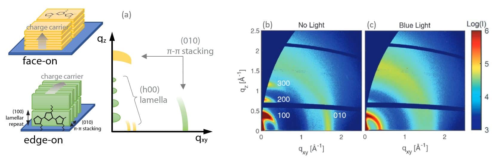
Fig. 2 (a) Typical GIWAXS scattering pattern that can be observed from a combination of edge-on and face-on phases. Note that the color code indicates the origin of each pattern. Image adapted from Ref. [5] (b, c) GIWAXS data recorded on P3HT thin films deposited on silicon substrate and treated with blue light or untreated. Credit: Adv. Funct. Mater., 2023, DOI: 10.1002/adfm.202212835.
In this study, both in-plane and out-of-plane lamellar (100) reflections have been analyzed as a function of applied light treatment. As shown in Figure 3 (a), samples treated with green and blue light exhibited an intensity reduced by half and a maximum intensity at lower qz values compared to the ones with dark or red light treatments. These observations reveal that treating the P3HT films with green and blue light will result in an increase of the real space lamellar packing distance as well as a decrease of both the crystallinity and the edge-on oriented aggregates. The decrease in crystallinity was also confirmed by atomic force microscopy measurements (AFM) which showed a decrease of surface roughness in samples treated with green and blue light.
When looking at the in-plane component however the opposite trend is observed (see Figure 3 (b)). The measured intensities increase significantly (approximately 4-fold) in films treated with green and blue light. This points toward a drastic increase in the fraction of aggregates oriented face-on with respect to the substrate.
The distribution of lamellar stacking orientations with respect to the substrate can also be quantified from GIWAXS measurements. As shown in Figure 3 (c), photoexcitation with green and blue light results in a significantly higher fraction of face-on polymer chains. At the same time, dark and red light treatment yield predominantly edge-on oriented crystallites.
When analyzing the real space in-plane lamellar stacking distance, calculated from GIWAXS measurements (shown in Figure 3 (d)), it is evident that a less efficient packing (larger lamellar stacking distance) is obtained when samples are exposed to green and blue light.
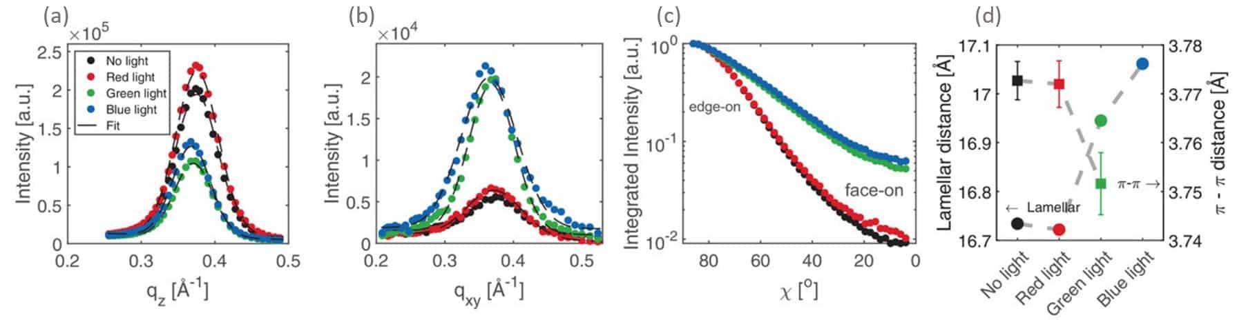
Fig. 3 Line integration of (a) out-of-plane and (b) in-plane lamellar (100) peak and Gaussian fit. (c) Integrated lamellar signal showing the orientation of the polymer planes with respect to the substrate: 90o corresponds to out-of-plane orientation (edge-on) while 0o corresponds to in-plane orientation (face-on). (d) Out-of-plane lamellar distances and in-plane π- π stacking distances for each light treatment. Note that no in-plane π- π stacking distance was observed following the blue light treatment. Credit: Adv. Funct. Mater., 2023, DOI: 10.1002/adfm.202212835.
Influence of morphology on the electrical properties of organic semiconductors
In terms of conductivity, the two groups of light treatment produce again significantly different properties. While no and red light treatments favor in-plane photo conductivity, blue and green light treatments will result in predominantly out-of-plane charge transport (as depicted in Figure 4). Knowing that in polymers conductance is limited by the inter-chain transport, this can be directly correlated with the change of morphology from edge-on to face-on induced by the two types of light treatment as revealed by GIWAXS.
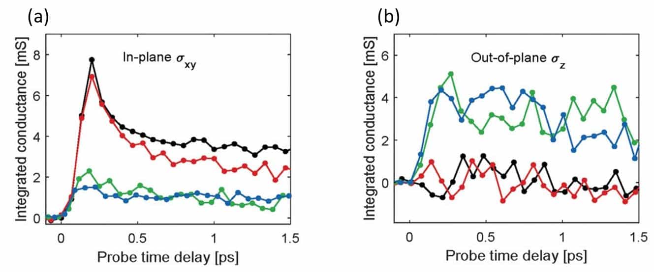
Fig. 4 Spectrally integrated (a) in-plane and (b) out-of-plane sheet conductivity extracted from full 2D time-resolved terahertz spectroscopy (TRTS) scans at normal incidence and at 45o incidence respectively. Credit: Adv. Funct. Mater., 2023, DOI: 10.1002/adfm.202212835.
For organic photovoltaics applications employing P3HT thin films a careful consideration of the orientation of P3HT crystallites in relation to the reference plane (bottom electrode) represented by substrate surface is necessary. The anisotropic conductivity of P3HT is higher along the backbone chains and the π-π stacking in the edge-on configuration, making it more efficient for charge transport parallel to the substrate surface. At the opposite end, the edge-on orientation with perpendicular staking will suffer from a reduced exchange of charge carriers with the electrodes. Therefore, in OPV applications, the face-on orientation is preferred as it allows for better exchange of charge carriers with the electrodes.
Conclusions
This study demonstrates that the thin film morphology of P3HT can be modified by applying different light treatments during deposition. Moreover, it shows that manipulating the packing behavior of P3HT in this way can be used as a tool to achieve the desired electric performance of these organic semiconductors thin films.
In this regard, GIWAXS proved to be an excellent tool to study the structural variations of thin films exposed to different photoexcitation treatments which in turn can be correlated with the different functions. Most notably it showed that applying blue or green light treatment during roll-to-roll slot-die coating yields predominantly face-on oriented crystallites, orientation which is favourable for OPV applications as it allows for better exchange of charge carriers with the electrodes.
The research was originally published in the following article: [3] Sørensen, M. K., Gertsen, A. S., Fornari, R. P., Zhou, B., Zhang, X., Jepsen, P. U., … & Andreasen, J. W. (2023). Manipulating organic semiconductor morphology with visible light. Advanced Functional Materials, 2212835.
[1] Myers, J. D., & Xue, J. (2012). Organic semiconductors and their applications in photovoltaic devices. Polymer Reviews, 52(1), 1-37.
[2] Martín-Palma, R. J., & Martínez-Duart, J. (2017). Nanotechnology for microelectronics and photonics. Elsevier.
[3] Sørensen, M. K., Gertsen, A. S., Fornari, R. P., Zhou, B., Zhang, X., Jepsen, P. U., Stanzani, E., Yun, S., Fernández Castro, M., Schwartzkopf, M. & Andreasen, J. W. (2023). Manipulating organic semiconductor morphology with visible light. Advanced Functional Materials, 2212835.
[4] Müller‐Buschbaum, P. (2014). The active layer morphology of organic solar cells probed with grazing incidence scattering techniques. Advanced materials, 26(46), 7692-7709.
[5] Osaka, I., & Takimiya, K. (2015). Backbone orientation in semiconducting polymers. Polymer, 59, A1-A15.